This site uses cookies to give you the best experience on our website and for site operation and analysis.
For more information about the use of cookies on this site, please review our cookie policy in our Terms of Use.
To help us provide you with better information, we ask that you accept the collection and use of cookies.
X-MININGX-TALK Vol.4
The Future Prospect of Printed Electronics
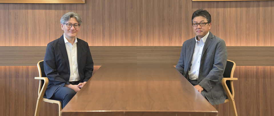
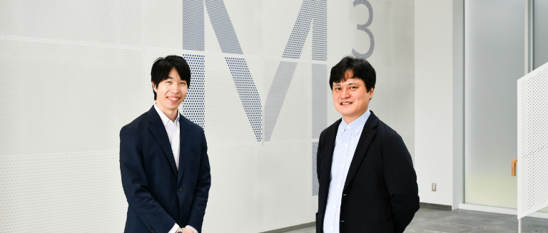
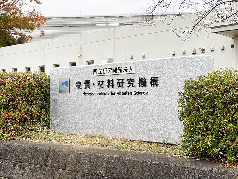
Dr. Minari, a leading authority on printed electronics technology in Japan, is conducting research at the National Institute for Materials Science (NIMS). While there are growing needs for semiconductors and peripheral materials following the spread of IoT technology, he is working toward the development of printable materials using copper powder with an eye toward the production of low-cost and zero waste organic semiconductor devices. Naoki Yamaoka who is involved in developing fine copper powder at our Niihama Research Laboratories asked Dr. Minari about the advantages of the printable copper material and the inside story of his research and development, and the venture business he established.
Profile
“Printable metal,” also beneficial from the viewpoint of the SDG
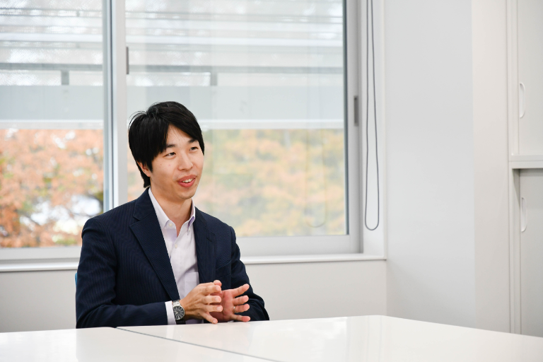
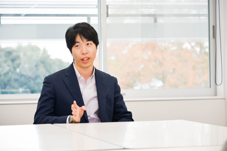
Yamaoka
Since I joined this company, I have been researching fine copper powder at Niihama Research Laboratories. I have a strong interest in the research and development of metal ink that is expected to be applied to the printed electronics materials Dr. Minari is concerned with, especially electrodes. Today, I would like to hear about your research. First of all, when did you start the current research?
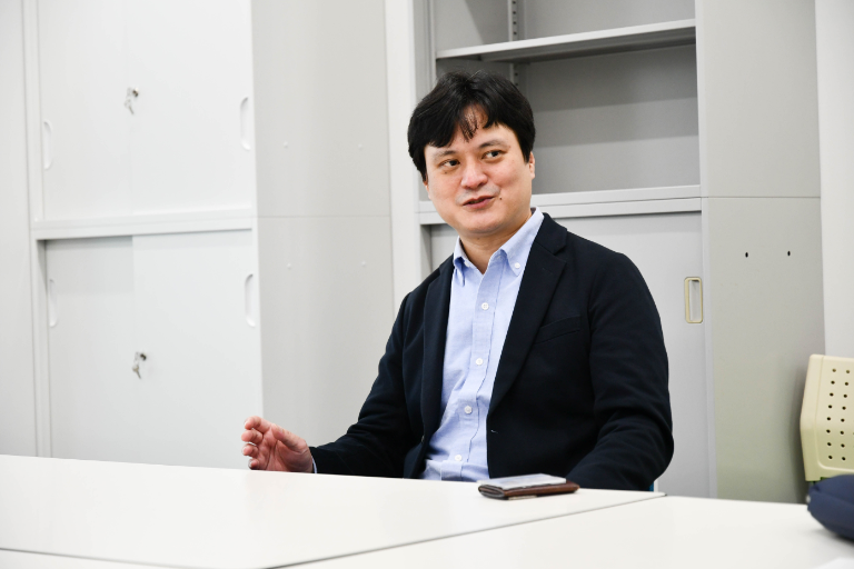
Mirinari
It was rather a long time ago. Around 2009.
Yamaoka
It’s been more than ten years since then! What first interested you?
Mirinari
I’ve been researching organic semiconductors since around 2007. One of the features of organic semiconductors is that you can dissolve them into a solution and apply them. The objective of my research is to create organic semiconductor devices, which consist of conductors, insulators, and organic semiconductors, by printing processes using their features.
However, while there are many printable semiconductors and insulators, we didn’t have a printable metal. I thought if we could create a printable metal, we could manufacture organic semiconductor devices with only a printing process.
Yamaoka
Other than printing, we can think of vapor deposition and spattering.
Mirinari
You are right. Those two methods are typical. Vapor deposition creates a film by heating to evaporate metal. In spattering, argon is blown on metal, metal atoms jump out and create a film. Both methods need a vacuum state. They also need large vacuum equipment and consume a significant amount of electric power. Which means it costs a lot!
On the other hand, printing is a simple process. Spattering and vacuum deposition cover the entire surface of the metal. Then unnecessary parts are removed by etching (dissolving) and only the board pattern remains. It is a great waste of resources. Printing in printed electronics, however, prints the materials only where they are required, which eliminates unnecessary processes such as etching.
Talking about the cost, a piece of vapor deposition equipment costs around one billion yen. However, introducing printing cost us less than a hundred million yen. Using a method such as ink jet printing, it is possible to realize on-demand manufacturing without a printing plate, so the cost scale is quite different.
Yamaoka
The process is very short and generates little waste. It can be recommended from the viewpoint of the SDGs.
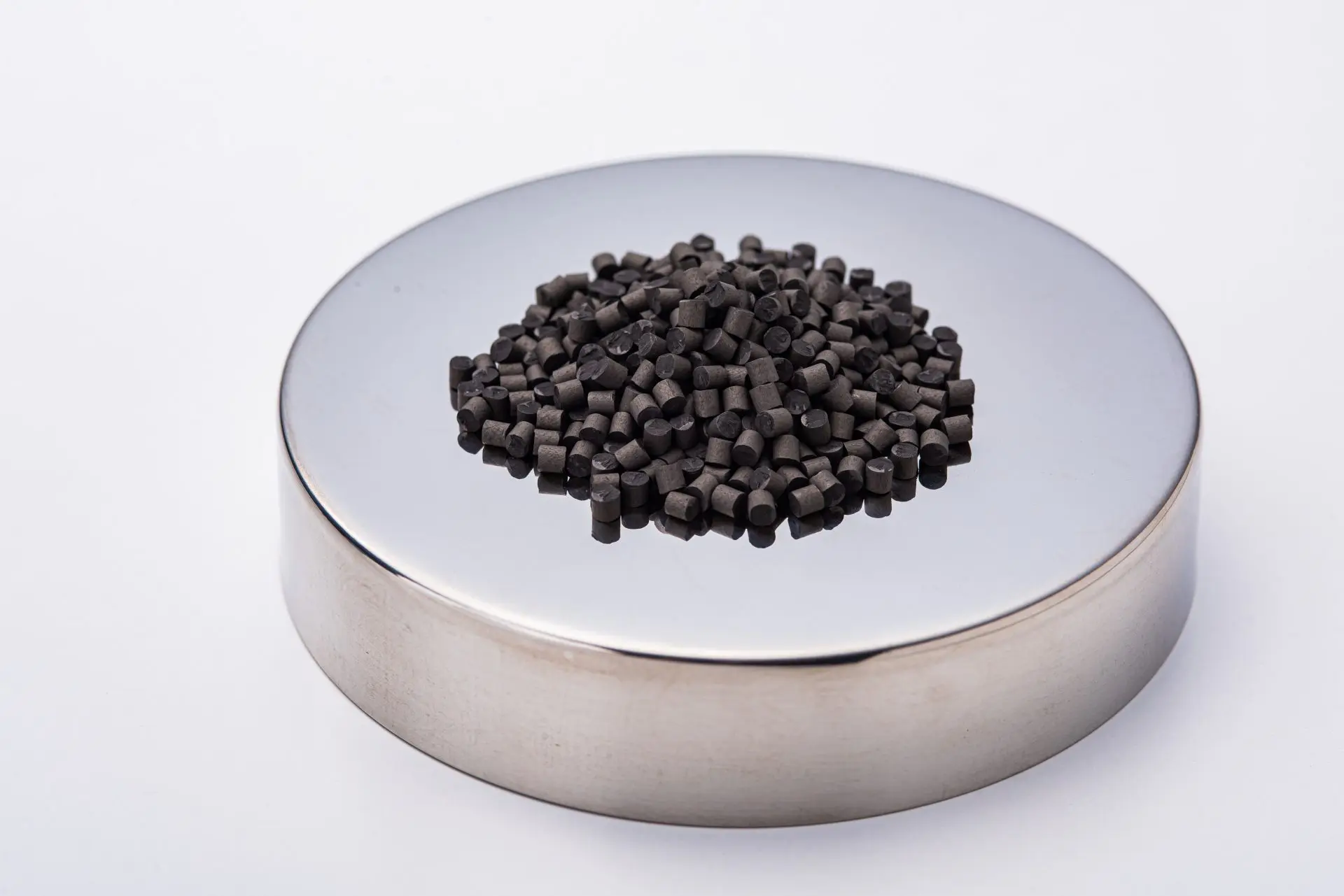
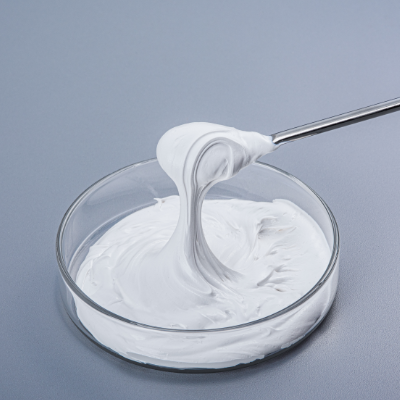
Copper powder has high conductivity but is cheap
Yamaoka
By the way, when was metal ink invented?
Mirinari
I think it existed before 2000. One reason for not being popular was that people did not think of using it to print circuits. And the other was because of its poor performance. The conductivity was not so good.
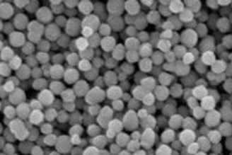
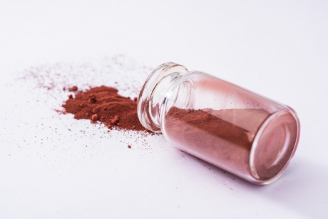
Yamaoka
Our company is currently developing copper powder that has good conductivity by sintering powder particles at relatively low temperatures. For the target applications, silver powder has been used for a long time. However, silver powder is expensive and has the drawback of tending to cause ion migration(*).
(*) Applying a voltage in a high-humidity environment causes metal in the electrodes to be ionized and deposited between the electrodes, resulting in a short circuit.
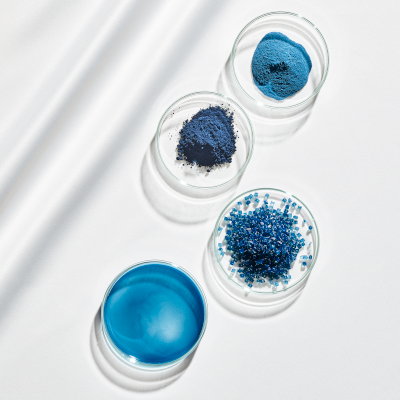
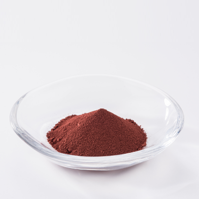
On the other hand, copper powder has high conductivity similar to silver, but is far cheaper. Efforts for using copper powder instead of silver powder have been made for years. However, copper powder easily becomes oxidized and is difficult to handle. The current research and development focuses on resolving this problem.
Mirinari
Another advantage of copper is good solderability. Silver tends to dissolve in solder, which makes it difficult to make a joint. Therefore, to form circuits with silver, we have to conduct other research on joining silver and solder.
Yamaoka
We think copper powder will be a solution to the problem with silver. We are planning to develop a raw material that substitutes copper powder for silver powder.
Mirinari
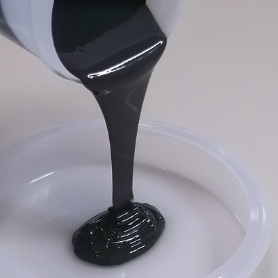
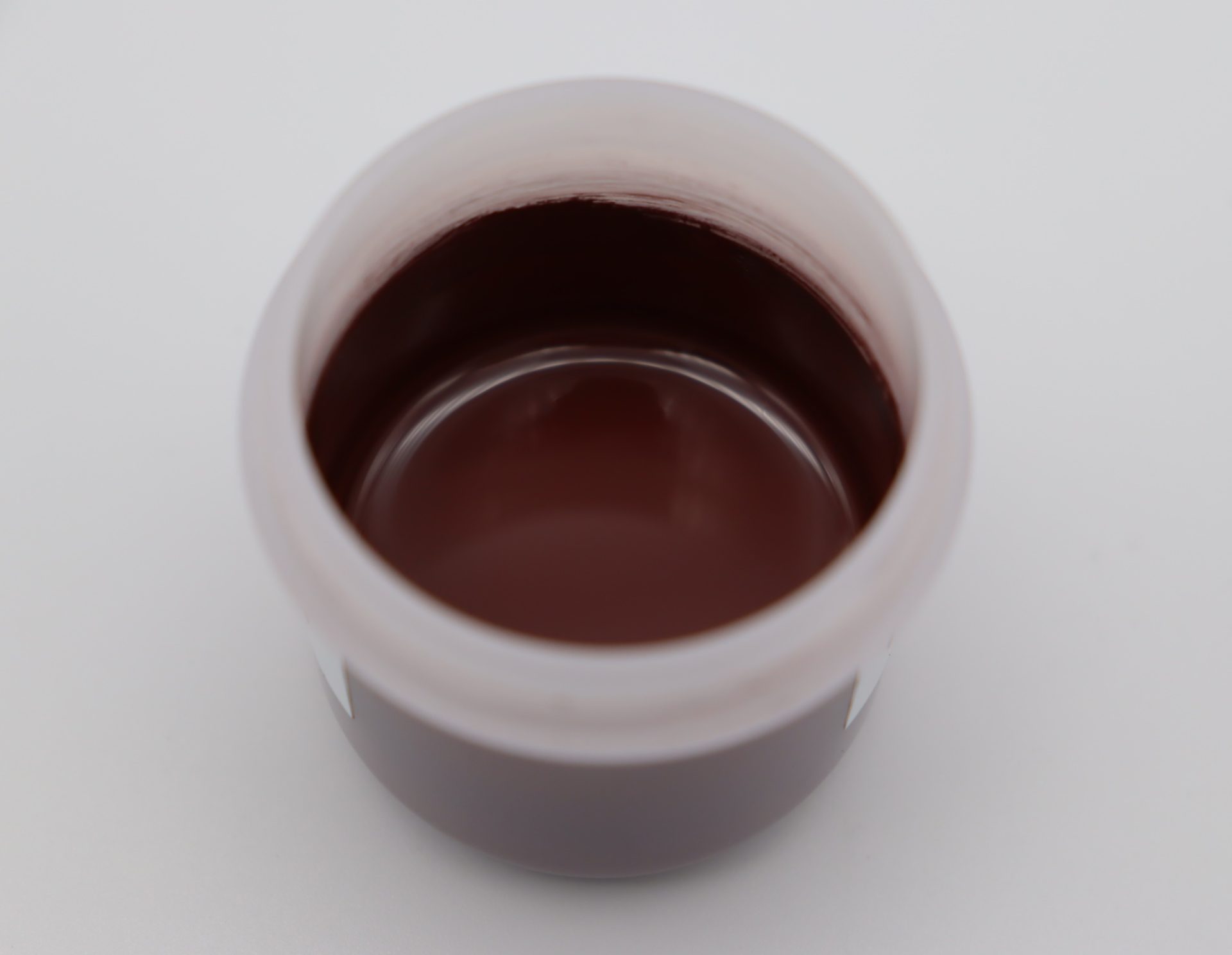
We are conducting research on the same principle as Mr. Yamaoka. The ink for printed electronics consists of nano particles or copper nano particles are exceptionally oxidable. Leaving a composition still, it will be oxidized in around one hour and become copper oxide ink. To resolve this problem, our laboratory is developing ink using copper complex ink in which copper exists stably as complex ions, and when it is heated, metal copper deposits. This ink is very stable. And if you take care of oxidation during sintering, the sinter films created with this ink have high conductivity. I think the issues are being resolved one by one.
Printed electronics is an indispensable technology for spreading IoT
Mirinari
Mr. Yamaoka, what do you think of the future potential of printed electronics?
Yamaoka
I think it will be an essential technology for IoT and its related fields. In order to expand the potential, we have to make efforts to raise the performance of the raw materials.
Mirinari
Spreading IoT means that electronics technology is introduced to areas where no such technology has been used before. To enable this, low-cost mass production technology is required.
We can say with assurance that printed electronics is highly suitable for IoT. In the age where various devices are imbedded in walls and interfaces are installed at many places, printing devices made by a new process are needed. And printed electronics will be demanded in such an age.
To realize this, it is essential to develop copper powder suitable for manufacturing metal ink. I hope Mr. Yamaoka will continue his research on copper powder.
Yamaoka
As a powder manufacturer, we will ask for an evaluation of the characteristics of conductive powder by many customers and research institutes, and continue modification based on their feedback. We are conversant with developing powder. But we do not have a wealth of know-how and experience in performance testing and application. Dr. Minari’s development efforts are focused on the process. I hope you will give us advice on a continual basis.
Research philosophy changed after establishing a start-up
Yamaoka
In addition to your research at NIMS, you have established a start-up.
Mirinari
Yes. Fundamental research is a very important activity. However, if you don’t understand the needs, you cannot direct your research in the correct direction. After establishing the company, I hear from many people, including a variety of requests for research and development. These requests show the direction our research should go. A company must perform research facing that direction to sell their products. A business model is also required for realization. After establishing a company, I naturally think of things that I was not aware of in the laboratory. In principle, I have been conducting research for practical applications. Establishing a company directs our activities.
Yamaoka
Our company, the same. Developing with and without understanding the needs has different processes and results.
Mirinari
And I am usually researching processes. Materials can sell as you produce them, but it is not easy to sell processes. This is why we developed printing equipment and ink materials, and are running a business to sell them.
Yamaoka
From the viewpoint of a company, I think we have many things in common with a person who also runs a start-up. With a person like you who also runs a business rather than being solely dedicated to research, we think we can exchange opinions in depth.
Mirinari
After establishing a start-up, I learned to direct my research to the needs of companies. If a company requests us to develop xx using its copper powder, we can direct our research to that need. I had been conducting research only on the subjects I was interested in, some of which were not matched to the needs of companies. After I started a company, I think I can look ahead of development. That is the most significant change.
Yamaoka
I hope we can team up with Dr. Minari’s business in some way, and contribute to the realization of printed electronics, which will help lead to the achievement of the SDGs. Thank you for joining us today!
Videos about Flash-lamp sintering and laser sintering (YouTube)
One of the tests of sintering electrodes which were pattern-printed with the metal ink. (upper : by using flash-lamp, lower : by using laser)
* Recorded on December 2021.
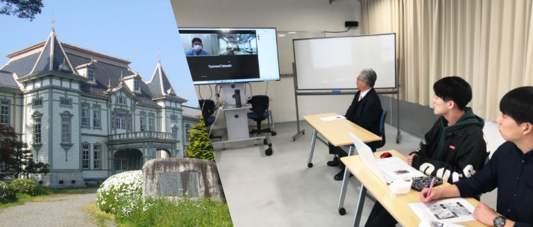
* Measures against COVID-19 infection were taken including measuring body temperature, sterilizing hands, ensuring sufficient ventilation, and keeping social distance. Masks were taken off only for photographs.
![[Wet-chemical synthesized metal powder] Ultra-fine nickel powders](https://crossmining.smm.co.jp/wp-content/uploads/m_np.webp)